


This website uses cookies so that we can provide you with the best user experience possible. Cookie information is stored in your browser and performs functions such as recognising you when you return to our website and helping our team to understand which sections of the website you find most interesting and useful.

FPGA Design Services
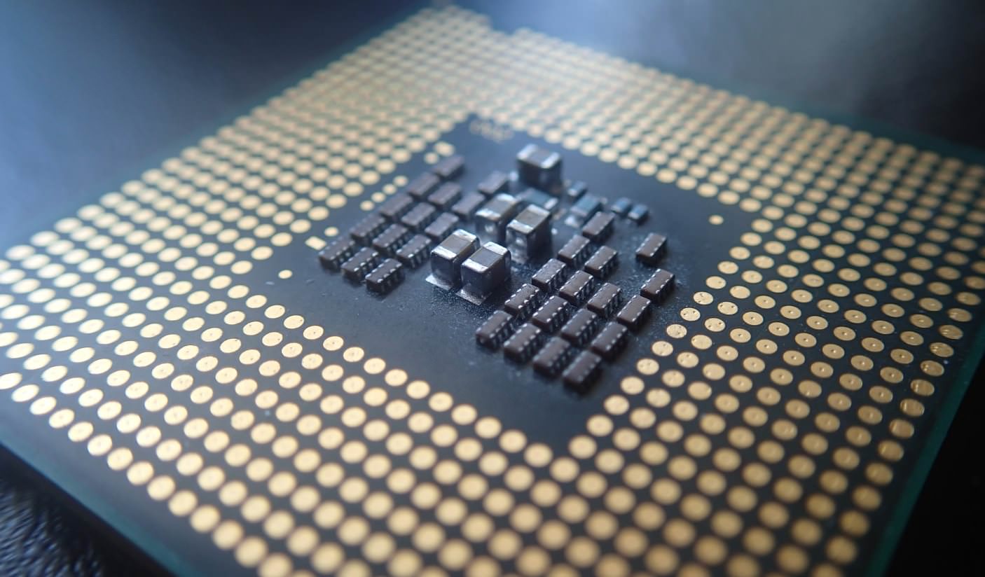
Unlike application-specific integrated circuits, FPGAs can be reprogrammed with hardware description languages after manufacturing. They are widely used in high-speed data processing systems, consumer electronics, telecommunication equipment, robots, systems that use neural networks, and more. Integra offers FPGA hardware design and verification, CPLD design, IP core configuration, and other services.
What we do
We provide field-programmable gate array (FPGA) design services for systems that use sophisticated features and advanced technologies: video and image processing, machine vision, and industrial networking. FPGAs contain millions of tiny logic cells and can perform almost any digital operation. We also offer complex programmable logic device (CPLD) design for simpler solutions. The team will build a prototype, test it, and help you arrange mass production if necessary.


What’s included

Architecture Development
The main goal of FPGA architecture development is to configure both logic and interconnections according to technical requirements. The architecture of an FPGA consists of programmable logic blocks that implement logic functions, programmable routing that establishes a connection between logic blocks, and input/output blocks for external connections.

FPGA Design Service
We use Hardware Description Languages (HDL) such as Verilog and VHDL to create a high-level representation of a digital circuit. To verify the functionality and performance of the circuit, we translate the HDL code into an RTL representation. Then the RTL design is converted into a gate-level netlist which is then mapped to the FPGA. Embedded Development Kit (EDK) implementation tools and reusable IP cores help us save months on development.

FPGA PCB Design
The Integra team can create advanced printed circuit boards that use FPGAs as co-processors or main controllers. This approach allows for achieving high computing power and parallelism. FPGAs can be used in systems with real-time capabilities, edge computing, solutions with multiple peripherals, and more. We will design the PCB, test the prototype, and help you arrange manufacturing.

FPGA Verification
During IP core development, the team runs post synthesis timing simulations, as well as functional and logical tests. We use various debugging tools and instruments (signal generators, scope, spectrum, and logic analyzers, as well as integrated logic analyzers) to test a finished device and verify logical elements, making sure each block of code can correctly process simple stimuli and each signal interface is correctly connected.

Configuration of IP Cores
We provide integration and connection of third-party IP cores or blocks of logic and customization of soft IP cores developed in Verilog or VHDL for custom FPGA and CPLD designs. The soft cores can include UART, CPU, Ethernet controllers, and PCI interfaces.

CPLD Design
Complex programmable logic devices are less flexible than FPGAs but have a simpler design. We suggest using CPLDs for solutions based on conventional microcontrollers or microprocessors that still require high-speed data processing for small tasks. CPLDs are cheaper and more energy-efficient than FPGAs. They have lower idle power consumption and are more secure because the design is stored in a built-in memory. They are also easier to route, which means the compilation time is going to be faster than it would be for an FPGA.

Have an idea?
SUBMIT A PROJECT
Our projects
Check Integra’s previous projects delivered within our CPLD and FPGA design services.

System and Application Software for Monochrome and RGB LED Matrix Display
The display integrates with traffic management systems. The software created provides effective communication with the traffic management system.

Custom Software Development for an Electronics Measurement Device
We designed data transmission and software licensing mechanisms, test and measurement apps, apps for calibration and streaming, and other software.
A USB Keylogger for Recording Keystrokes Typed on Any PC
The device records the data being transmitted by a keyboard. It captures every key pressed by a user and stores this information in a text file.
Awards


Why choose Integra Sources
Innovative problem-solving skills, in-depth expertise, and enthusiasm make us a strong partner for hardware and software development.
LEARN MORE ABOUT OUR WORKFLOW

Integration
- Adaptation to customers’ management systems
- Integration into customers’ development processes

Flexibility
- Flexibility in development
- Flexibility in communication

Communication
- High level of communication
- Personal account management
- Legal security guarantee

Transparency
- Transparency in development processes
- Customer’s dashboard
- Clear timelines
Industries
LEARN MORE ABOUT THE INDUSTRIES WE WORK WITH
Consumer Electronics
Consumer devices, wearables, smart home solutions, desktop, mobile, and web applications.

Power Electronics
BESS and BMS solutions, charging systems, electric motor controllers, power conversion.

Extractive Industry & Manufacturing
Industrial automation, industrial IoT, computer vision, tracking solutions, wearables, industrial UAVs.

Healthcare
HMIs for medical equipment, wearables, computer vision and AI-based diagnostics solutions.

Logistics & Transportation
Location and status tracking for freight and vehicles, warehouse robotics, order and warehouse management systems.

Science & Education
Measuring and testing equipment, programmable robots, e-learning solutions, curriculum management systems.

Agriculture
UAVs and autonomous robots, soil analysis and climate control systems, solutions for precision agriculture, asset tracking.

Entertainment
Multimedia solutions, video streaming systems, desktop and mobile applications, drones.

Robotics
Hardware and software, electric motor controllers, computer vision algorithms, AI solutions.
We've worked with
enterprises
and
startups
from Europe, the USA, Australia, and Asia


Our tech stack
Languages
OS
FPGA Families
Altera Cyclone, Altera MAX, MicroBlaze, PicoBlaze, Xilinx, Xilinx Spartan Series, Zynq.
IDE

ECAD Software
Interfaces
CF/MMC/SD, DVI, Ethernet, HDMI, I2S, LAN, LCD, LPC, PCI, PCI-E, SATA, USB, SPI, RS-232, RS-485, CAN, I2C, UART, MIPI, DSI, MODBUS.
Wireless Technologies


Math and Simulation Tools
Vendors
Testing and certification
Integra’s services include thorough testing, debugging, and pre-certification steps. Our experts carefully review the certification requirements applied to the product and stick to them at all development stages. We provide all the necessary documentation for further electronics certification and software audits.
DISCUSS A PROJECT
Show more
Explore our workflow
GO to workflow page
1
We get acquainted with the concept of the future device and sign a non-disclosure agreement. The team gathers project requirements, studies relevant documents, and analyzes rival products on the market. At this phase, a preliminary project evaluation is made.
2
We contact the customer to confirm the project requirements. Then we create a technical specification and set a budget and deadlines.
3
We make the final evaluation of the project, make up a team, and schedule its workload.
4
We sign a contract for FPGA or CPLD design. The team gets to work.
5
There are two possible options. One is to use a devkit to program an FPGA/CPLD first and then design a suitable printed circuit board for it. The other option is to design a PCB with a powerful enough FPGA/CPLD and then program it. After that, the team either leaves the prototype unchanged or replaces the FPGA/CPLD with a less expensive alternative.
6
The team tests all the functions of the device. We check its performance under corresponding operating conditions and run some tests required for product certification. If necessary, the product is then modified.
7
After the tests, we finalize the documentation necessary for mass manufacturing, including the bill of materials, Gerber files, etc. We can also prepare manuals if the product is designed for in-house use.
8
When the development process is finished, customers can enjoy a free warranty period. During this time, the team will fix any bugs and defects in the product.
Reviews
“Integra Sources delivers to the highest standards, not only in the physical work they produce but also in their communication and documentation. It has by far exceeded our standards. They researched the project in-depth to better understand our goals - that really impressed us.”

Richard Youden
Owner and CEO, Eau Rouge Engineering
“Integra Sources’ extensive preparaion beforhand helped give me confidence that we chose the right partner. Despite the time difference, they are able to stay in constant communication. Integra’s dedication to the project has led us to develop an ongoing relationship.”

Christophe Baudia
CEO at GeoMoby
"The database has satisfied all scope requirements. The upgrades have improved communication and performance. Team strengths include accessibility and problem-solving and they are unafraid to research problems and develop their own solutions. Integra demonstrated strong management skills when they manage our servers for a week during an important trade show; we showcased our product at the event. Communication channels are always fluid and straightforward."

Eduardo Ruiz
Founder & CEO at Ruiz Aerospace Manufacturing
Show more
Frequently Asked Questions
Read this information to better understand FPGA PCB design.
What do I get when the project is finished?
Do you do receipt inspections of the components you receive?
What about intellectual property rights?
What IP cores do you use?
Do you validate FPGA firmware?
What FPGA chips do you work with?
Have you worked with SoC systems that use both FPGA and CPU?
What is the main difference between ASIC and FPGA?
Could you help me choose an FPGA chip for my project?
Can you design a custom board for an FPGA?
Will you test my device?
Can you guarantee the quality of the product?
Can you help me with certification?
What is the minimum completion time?
Can you help me with enclosure design?
Who are your customers?
Related services
Check out other services we provide.

Kernel and Driver Development
We implement device driver development projects for Linux, Windows, and macOS and develop Linux kernel modules for embedded devices. The...
LEARN MORE ![]()
LEARN MORE ![]()

Printed Circuit Board (PCB) Design and Layout Services
Schematic design, PCB layout, and fabrication – we offer a complete set of services for implementing printed circuit boards.
LEARN MORE ![]()
LEARN MORE ![]()

Firmware Development Services
As a firmware development company, we have extensive experience with hardware, operating systems, low-level diagnostic and performance tools.
LEARN MORE ![]()
LEARN MORE ![]()